
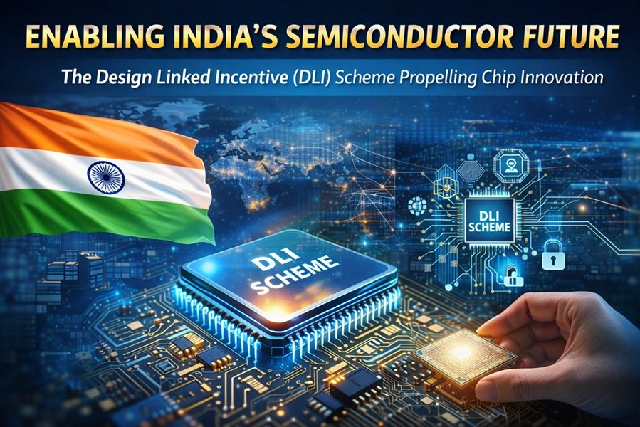
DLI Scheme: India’s Strategy to Become a Global Semiconductor Design Hub
India’s march toward technological self-reliance and global competitiveness has taken a decisive turn with the implementation of the Design Linked Incentive (DLI) Scheme — a strategic initiative designed to strengthen the domestic semiconductor ecosystem. In an era where digital infrastructure underpins economic progress, India’s policy focus on building robustness in semiconductor design reflects a long-term vision to break free from import dependence, foster indigenous innovation, and build a resilient technology industry.
Technology that fuels modern economies — from smartphones to electric vehicles, telecommunications to defence systems — depends on sophisticated semiconductor chips. While global supply chains are historically concentrated in a few regions, India is now reshaping its role by prioritizing chip design as a fundamental driver of value creation. According to the official release from the Press Information Bureau (PIB), the DLI Scheme is a core component of the broader Semicon India Programme, aiming to cultivate a competitive, self-sufficient semiconductor design ecosystem in the country. (Press Information Bureau)
Why Chip Design Matters
In the semiconductor value chain, design represents the most critical and high-value segment. Although manufacturing fabs produce physical chips, the real intellectual property and strategic advantage lies in the design phase. Semiconductors designed with innovative architecture and embedded intelligence account for a significant portion of the product’s economic value, often up to 50 % or more of the total. (Press Information Bureau)
Countries or companies that control the design layer wield considerable influence over global technology standards. Without strong domestic capabilities in semiconductor design, a nation remains inherently dependent on international suppliers even if fabrication occurs locally. Recognizing this, the Indian government is channeling substantial policy focus and resources into nurturing a homegrown fabless design ecosystem that champions innovation, intellectual property ownership, and strategic autonomy. (Press Information Bureau)
The Design Linked Incentive (DLI) Scheme: Core Features
Launched under the Ministry of Electronics and Information Technology (MeitY) as part of the Semicon India Programme, the DLI Scheme offers a comprehensive suite of incentives aimed at catalyzing India’s semiconductor design competencies. Its purpose is clear: to transform India into a preferred global hub for chip design innovation. (Press Information Bureau)
Targeted Financial Incentives
The scheme provides targeted financial support to startups, MSMEs, and domestic companies engaged in semiconductor design:
- Product Design Linked Incentive: Offers reimbursement of up to 50 % of eligible expenditure, capped at ₹15 crore per application.
- Deployment Linked Incentive: Provides incentives equivalent to 4 – 6 % of annual net sales turnover for a period of up to five years, capped at ₹30 crore per application — contingent on successful market deployment of the design.
These incentives are structured to reduce upfront financial barriers and encourage sustained investment in design innovation, enabling Indian firms to compete effectively on the global stage. (Press Information Bureau)
Access to Shared Design Infrastructure
A standout feature is the establishment of national semiconductor design infrastructure, particularly through:
- The ChipIN Centre, led by the Centre for Development of Advanced Computing (C-DAC), which provides remote access to advanced Electronic Design Automation (EDA) tools.
- A comprehensive IP Core repository, enabling developers to integrate pre-validated functional modules into their designs.
- Prototyping support under Multi-Project Wafer (MPW) arrangements, and post-silicon validation support — essential steps to transition a design from concept to production.
This shared infrastructure dramatically lowers the cost threshold for startups and MSMEs, leveling the playing field and accelerating innovation. (Press Information Bureau)
Tangible Outcomes: Building India’s Chip Design Ecosystem
Since its inception in December 2021, the DLI Scheme has begun producing measurable results:
- Over 95 companies have gained access to high-end design tools and frameworks.
- The national EDA Grid — a centralized semiconductor design platform — has logged over 54 lakh usage hours, indicating strong adoption across academia and industry.
- Early stage outputs include 16 completed chip design tape-outs, 10 patents, and the development of over 140 reusable semiconductor IP cores.
- Over 1,000 trained engineers are now actively contributing to design activities, strengthening India’s talent base in this specialized field.
These accomplishments spotlight an ecosystem transitioning from dependency to capability — a necessary shift if India is to be counted among the world’s technological innovators. (Press Information Bureau)
Success Stories: Innovation in Action
The Scheme’s impact is best captured through the success of individual companies:
- Vervesemi Microelectronics has developed a portfolio of over 110 semiconductor IPs, spanning diverse applications from consumer electronics to automotive components.
- InCore Semiconductors focuses on indigenous RISC-V microprocessor cores, emphasizing performance and scalability for embedded systems.
- Netrasemi has taped out India’s first advanced AI-capable System-on-Chip (SoC) at a cutting-edge 12 nm node, showcasing India’s growing sophistication in design.
- Aheesa Digital Innovations and AAGYAVISION are pushing boundaries with broadband SoCs and advanced radar-on-chip technologies, respectively.
These examples represent more than commercial ventures — they signify India’s ascendancy in developing foundational technologies that underpin future digital systems. (Press Information Bureau)
Strategic Implications for India’s Tech Ecosystem
The DLI Scheme marks a decisive shift in India’s semiconductor strategy — from being a consumer of technology to becoming a creator and exporter of high-value semiconductor IP and designs. By focusing on design innovation, the country gains several strategic advantages:
- Reduced import dependence on critical semiconductor technologies.
- Strengthened intellectual property ownership within Indian industry.
- Enhanced global competitiveness in high-tech manufacturing and systems.
- Expansion of skilled employment and opportunities in the deep-tech sector.
Ultimately, the DLI Scheme serves as a strategic enabler — laying the foundation for a resilient, self-reliant, and future-ready semiconductor ecosystem capable of powering India’s digital ambitions. (Press Information Bureau)
Reference
Source: “Design Linked Incentive Scheme — Catalyzing India’s Semiconductor Design Ecosystem,” Press Information Bureau, Government of India. (Press Information Bureau)